

The Knowles Precision Devices DLI brand of technologies are designed to address the complex challenges of implementing high-performance mmWave filters across the widest range of specifications. Our Microwave Product Catalog covers how to select the best catalog or custom components for your application needs, while our new Microwave Products Guide provides valuable information and recommendations for how to work with our DLI brand microwave products once you have the components in hand.

If you are not familiar with our DLI brand, these devices utilize thin film technology and our specialized ceramic materials, which provide a substrate with enhanced properties compared to traditional substrates such as Alumina. We help customers achieve the best performance for their thin film applications by using precise manufacturing techniques to apply thin metal layers to create a pattern.
The Microwave Product Guide includes general information that is pertinent to all DLI brand devices as well as detailed recommendations for certain device types and/or configurations. In this blog post, we will dive into the details on one of those device types by exploring the anatomy of our DLI brand filters and stencil design recommendations.
The Anatomy of a DLI Brand Filter
To get a better understanding of how to incorporate your DLI brand filter into your device, let’s first look at the anatomy of our filters by using Figure 1 as a guide.
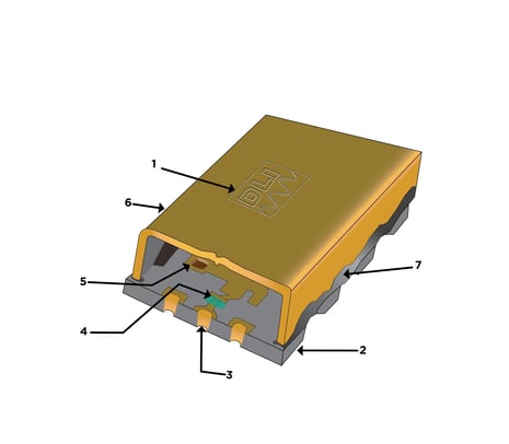
- The Knowles Precision Devices’ DLI brand logo and product identification are etched on the top of the filter.
- This is the ceramic substrate.
- Input/output (I/O) castellations are included on both ends of the board (note, the second I/O castellation at the other end of the filter is not visible in this picture). Solder is meant to form a fillet at the bottom of the castellation. Around 70 percent is acceptable because excessive solder flow onto the topside of the ceramic substrate will risk degradation of RF performance.
- This is the solder dam deposit, which may vary from this example in color, size, or shape. The solder dam deposit is included in many filter designs to mitigate the risk of solder flow on the top of the ceramic substrate.
- These are interior plated vias.
- The integrated shield is a gold-plated 430SS stainless steel three-sided cover.
- This is the high melting point solder used for cover attachment. We use RoHS-compliant solder per exemption 7a. The composition of the cover is 92.5 percent lead, 5.0 percent tin, and 2.5 percent silver (Indalloy151). The melting point of the cover is between 287 ˚C and 296˚C. Note that during the cover attachment process, the solder may form an irregular pattern on the side of the cover and bottom side of the part. This is normal and does not interfere with the subsequent surface mount soldering process.
DLI Brand Filters: Stencil Design Recommendations
All devices in our Microwave Products Catalog have a recommended PCB layout, which is available in the design files on our website. Stencil designs should be based on the PCB layout following these steps:
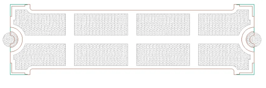
- Make a circular deposit at each I/O point with a diameter matching the annular ring diameter on the bottom of the part as shown in Figure 2.
- Windowpane the ground plane targeting 70 to 80 percent area coverage with deposits of a similar size. Maintain at least 10 mils distance between the I/O deposit and all ground plane deposits.
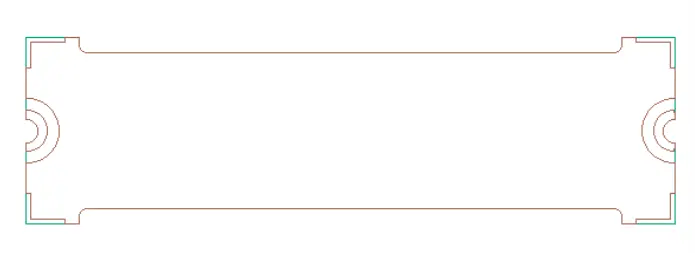
Outline of the bottom of the part where the orange outlines represent the ground pad and I/O points.
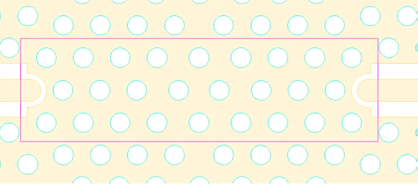
PCB layout with vias in green and the limits of the solder mask in pink.
Bottom of part with grey solder areas.
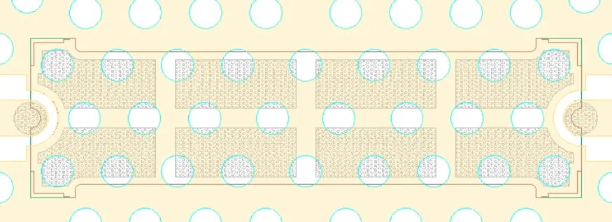
PCB layout with overlaid part including grey solder areas.
Figure 2. Four diagrams of the part and PCB layout with each diagram labeled above.
Below are some additional notes for best practices for PCB layout stencil designs:
- If a design has internal vias, which are noted in the bottom view drawing, you should align the panes of the ground plane stencil design to avoid deposits in the same position as the vias.
- Solder mask patterns on the PCB shall not extend under the body of the device (2-3 mils clearance preferred from perimeter of device).
- I/O deposits should follow the area ratio rule of >0.66 to avoid variation in solder deposition (see the chart below where acceptable sizes are in green and typical sizes are bold)
Area Ratio = Area of the Aperture/Area of the Walls > 0.66
Area Ratio Decision Chart
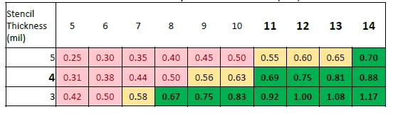
Circle aperture diameter is noted in mil.
