

As the RF spectrum becomes more crowded and the number of bandwidth battles grows each year, RF designers are looking for innovative designs that minimize interference while also increasing signal transmission power. Since phased arrays can efficiently maximize gain and signal directivity and minimize interference for both Tx and Rx, adoption of this architecture by RF designers is growing. This means RF designers are also on a quest for phased array filtering options that can help meet the size, weight, and power (SWaP) needs and performance demands required by today’s RF applications. As a result, our engineers have spent a significant amount of time working on an innovative approach that can meet this seemingly impossible combination of requirements.
Options for Phased Array Filtering
To understand the innovative phased array filtering approach our engineers are currently working on, it’s first important to understand that filtering in a phased array can be done in the following three positions (which are all shown in Figure 1):
- Position three (F3) – This filtering is done between the mixer and the feed network to suppress LO, image, spurious, noise emissions, and incoming interferers that accidentally fall in the IF band after the mixer. This is the most common approach today.
- Position two (F2) – This approach is best for applications where low loss is less critical and the application needs to filter incoming interferers relatively far from the desired frequency band.
- Position one (F1) – Filtering at F1 is challenging because it is done behind or in combination with the antenna element, but it does not allow any of the additional harmonics or noises from the last stage amplifier to pass through.
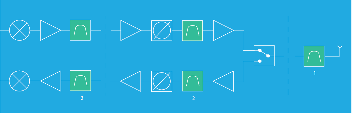
Figure 1. This single TRX path shows where filters could be added at positions 1, 2, and 3.
A Brief Background of F1 Filtering and the Challenges with mmWave Applications
The concept of F1 filtering is not new. In the Cold War Era, UHF phased arrays the size of a commercial building were used mainly for military applications such as radar and missile detection. In these applications with no SWaP constraints, filters at F1 maximized system performance by minimizing interference and reducing system noise. And today, filtering at F1 in the S and C bands below 5 GHz for Wi-Fi and cellular services and ISM radio bands is common. But at higher frequencies, especially above 10 GHz, F1 filtering solutions require different approaches. This is because the technology needed to minimize path loss often conflicts with packaging and integration requirements at mmWave frequencies.
But even given these challenges, it’s important to explore the possibilities of incorporating filters at F1 since this approach places the filter at the beginning of the Rx path and the end of the Tx path of the array, which offers multiple benefits versus filtering at F2 or F3. First, this configuration promotes radiation efficiency because it minimizes loss in the path between the last amplifier and the antenna. As a result, the area of the spectrum the application is most sensitive about is cleaned up significantly, spectral noise is reduced, and the link budget is improved, resulting in overall efficiency and performance gains.
Filtering at Position 1: A Difficult, But Not Impossible, Task
Recently, our engineers developed a concept for F1 filtering at higher frequencies that provides excellent performance while also maximizing SWaP. This concept builds on existing Knowles Precision Devices’ technology that offers the best tolerance, Q, and integration capabilities for filtering at F2 and F3 positions. Our design goes beyond using typical surface mount or board-integrated technologies, instead using 3D elements to create a panelized filter array (Figure 2).
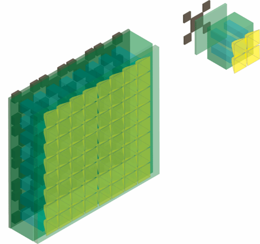
Figure 2. In this design, horn antenna elements are constructed on one side of the panel, while the feed to each antenna element from the ICs on the back of the panel is designed as an in-line filter, minimizing space and transitions.
Early prototypes of this 3D panel array filtering solution have demonstrated the ability of this concept to scale in size up to 256 elements, with the possibility of larger arrays in the future. Smaller array blocks such as 2 x 2 or 4 x 4, can also be assembled in tiles, which lends itself to scalable array architectures. As a result, we know our proposed filter array solution is a paradigm shift for mmWave phased arrays that will allow RF designers to integrate high-performance, low-loss filters directly behind the antenna elements with integrated feeds and transitions.
To see how this innovative 3D panelized filter array solution can be a viable solution for applications ranging from lower-frequency military and aerospace devices that need to focus on SWaP concerns to densely packed mmWave devices, download our latest whitepaper, Reduce SWaP, Increase Performance of Phased Arrays with an Innovative Filtering Approach.