

To provide a better understanding of build-to-print in general and the breadth of our offerings, as well as how our thin-film technology can benefit your applications, we’ve put together a Build-to-Print Basics series. Part 4 provides an overview of our process and the topics our applications engineers review with clients to kick-off any build-to-print project.
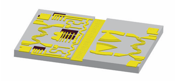
Knowles Precision Devices offers comprehensive in-house capabilities for build-to-print applications. In this post, we take a closer look at the process we follow for build-to-print projects. Below is an overview of our process and the topics our applications engineers review with clients to kick-off any build-to-print project.
Substrate Material
First and foremost, we need to determine the most appropriate substrate material for an application. We stock the most common materials including Alumina, Aluminum Nitride, high-dielectric Titanates, Quartz, and Sapphire, and also have a wide-variety of custom ceramics. We can work with materials of a standard thicknesses from 10 to 40 mil in increments of 5 mil and offer surface finishes of “as fired”, lapped, or polished. In post 5, we will discuss more details on substrate materials.
Plated Thru Holes and Filled Vias
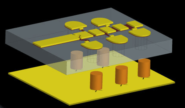
Next, we need to have a conversation about the size, location, and material required for any plated thru holes or filled vias needed. Our manufacturing facility has multiple CO2 lasers to precisely control the drilling process for thru-holes and vias. Our Cu filled vias have been space and flight qualified by multiple customers and are widely used to achieve cost-effective, high-volume designs at a fraction of the cost of Au filled vias (Figure 1).
Sputtering
We maintain several multi-target sputter machines with commonly used metals for quick-turn standard delivery without a premium. Adhesion metals consist of Ti and TiW as well as Cr, NiCr and TaN. Resistors using TaN and NiCr are standard. Barrier metals consist of Ni, Pd, and Pt, as well as Cr and TiW. Conductors using Cu, Au, and Al are all standard. High-power conductors using Cu or Au are also available. Below is a list of proven metallization schemes that we recommend and will elaborate on more in post 6:
S1 - 300 Å TiW, 50 µin NiV, 100 µin Au
S2 - 300 Å TiW, 50 µin NiV, 300 µin AuSn
S5 - 300 Å TiW, 100 µin Au
S5A - 300 Å TiW, 200 µin Au
S7 - 300 Å TiW, 6 µin Pt, 100 µin Au
S10 - 300 Å TiW, 100 µin Au, 50 µin Ni / 3-6 µin Au
S10A - 300 Å TiW, 200 µin Au, 50 µin Ni / 3-6 µin Au
S12 - 300 Å TiW, 100 µin Cu, 50 µin Ni / 3-6 µin Au
S12A - 300 Å TiW, 200 µin Cu, 50 µin Ni / 3-6 µin Au
S19 - 50 Ω/ sq. TaN, 300 Å TiW, 100 µin Au
Photolithography
Today, some RF circuit designs are approaching the need for the same demanding standards used in the semiconductor industry. Therefore, we have advanced our process to include multiple aligners and use a variety of tooling to manufacture designs to exacting standards. Using a combination of Mylar and glass tooling, we can manage the cost of non-recurring engineering while still providing features as small as 0.0004" (10 um) to tolerances of ±0.0001". We also use selective plating to achieve wire bond or solderability in the standard schemes described above.
Electroplating
For applications where photolithography is not needed, we offer environmentally friendly electroplating capabilities. We offer two different processes depending on client needs – one that is an etch back process and one that uses a sputter seed layer, etch artwork, and then a build-up plating process for the remaining layers.
Dicing
For customers that require high-volume production, we have ever-growing dicing capabilities to provide high-volume throughput of parts as small as .015” x .015 up to a thickness as large as 90 mil. Since dicing is typically a bottleneck in many operations, we strategically expanded this part of our manufacturing process to ensure throughput matches the balance of the operation.
Laser Trim
For applications where resistors have tighter tolerances below our standard bake-in tolerance of ±10 percent, we have resistor trimming available . This could include high-volume throughput for chip resistors, attenuators, and complex circuits. Plunge cut, scan cut, microwave scan cut, ladder networks, and "copy trim" are all aspects of laser trim that can be incorporated into a design for tolerances as small as 1 percent. Additionally, laser cutting is available for areas within the part that need to be removed such as location pins or hard-to-fit parts with profiles that are not geometrically square.
Packaging
Finally, all devices need to be packaged when they are completed. We have comprehensive packaging options readily available including all types of waffle pack, bulk packaging options, and tape and reel services.
In several future posts, we will expand on many of these topics. In the meantime, you can check out the rest of our Build-to-Print Basics series posts to learn more about our build-to-print and thin film offerings or download the comprehensive Build-to-Print Ebook today.
