

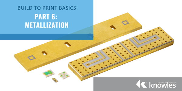
To provide a better understanding of build-to-print in general and the breadth of our offerings, as well as how our thin-film technology can benefit your applications, we’ve put together a Build-to-Print Basics series. Part 6 covers the various aspects of metallization that we consider to determine the best fit for our customer’s build-to-print applications.
Once the appropriate substrate is identified, the next critical parameter to evaluate is the selection of metallization. This includes making decisions on a variety of factors such as solderability, solder types, solder hierarchy, circuit attach, skin depth, conductivity, and thermal extremes. Typically, depending on what is decided, metallization ends up being the single largest factor in determining lead time and compatibility of processes.
Standard Metallization Systems
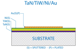
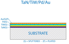
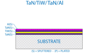
Standard metallization systems consist of materials for four different layers – resistor, adhesion, barrier, and conductor. Some of the common material schemes we recommend for the adhesion, barrier, and conductor layers include the following:
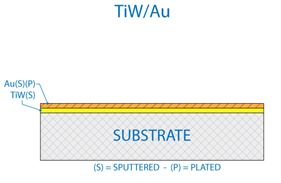
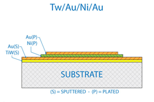
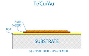
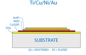
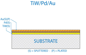
- TiW/Au, TiW/Ni/Au, TiW/Pd/Au and TiW/Cu/Ni/Au with TiW forming the main adhesion layer
- Ni or Pd (optional) functioning as a barrier layer for solderable devices
- Au or Cu as the main conductor, where Au can be fully sputtered or plated to various values of thickness to enhance skin depth and conductivity (discussed more below)
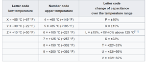
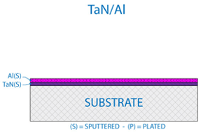
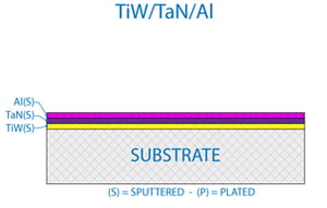
When it comes to the resistor layer, this layer is deposited before adhesion layers due to post processing requirements. TaN is the most common resistor material used because it offers well-established self-passivating characteristics. For applications where minimum resistor change over temperature extremes is critical, NiCr resistor films are a good choice. Various sheet resistance values are available depending on the resistor range for the overall design. More details on the typical values of various materials and characteristics of common combinations we use are included in Table 1 and Table 2 below.
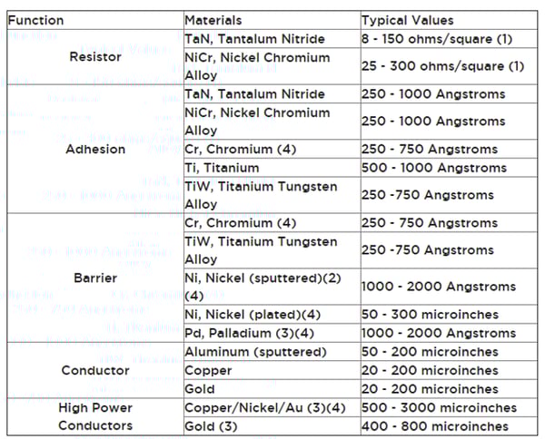 1 - Post heat treatment, 2 - Pure Nickel, 3 - Limited minimum feature size, 4 - Temperature limited due to metal diffusion
Table 1: This table shows the typical values for various materials commonly used for each layer.
Standard Metal Systems (RoHS Compliant)
|
|
Bondable |
Fine Lines |
High |
Solderable |
|||
|
Metal System |
Au/Wire |
Al/Wire |
< .002" |
Power |
Pb |
RoHS |
Au |
|
|
Y |
N |
N |
Y |
Y |
|
Y |
 |
N |
N |
N |
Y |
Y |
|
N |
 |
Y |
N |
Y |
Y |
Y |
|
Y |
 |
Y |
N |
Y |
N |
N |
|
Y |
 |
Y |
N |
Y |
Y |
Y |
|
Y |
 |
Y |
N |
Y |
Y |
Y |
|
Y |
 |
Y |
N |
N |
N |
Y |
|
Y |
 |
N |
Y |
N |
N |
N |
|
N |
 |
Y |
N |
Y |
N |
N |
|
Y |
 |
Y |
N |
Y |
Y |
Y |
|
Y |
 |
Y |
N |
N |
Y |
Y |
|
N |
 |
Y |
N |
N |
Y |
Y |
|
Y |
 |
Y |
N |
N |
N |
Y |
|
Y |
 |
N |
Y |
N |
Y |
N |
|
N |
 |
N |
Y |
N |
N |
N |
|
N |

Table 2. This table includes diagrams and additional functional details for common metallization systems we recommend for our build-to-print customers.
Adhesion Layer Thickness
To support the metallization schemes in Table 2, Knowles Precision Devices recommends best practices on adhesion layer thickness based on the design provided for review. To achieve the best possible metal adhesion for your design, consider the following recommendations for adhesion layer thicknesses for TiW for your design:
- 500 ± 250 Å (simple patterns/conductor only)
- 1,000 ± 250 Å (for plated thru vias and slots)
- 1,250 ± 250 Å (for filled vias)
If your design is different than the standard process considerations listed above or has special characteristics such as vias and edge castellations, we also can make custom recommendations that best suit your application needs.
Platting vs. Sputtering for Thicker Metals
Some designs need thicker conductors for skin depth requirements or to meet incorporated company standards. The common technique of sputtering can have several negative impacts at increased thicknesses. First, it is costly to deposit precious metals and then etch the circuit features. Second, thick sputtered structures that are subsequently chemically etched undercut the patterned resist due to the isotropic nature of the process. This results in a cross-sectional profile that is more trapezoidal than square.
Instead, structures thicker than 100µ" benefit from using a selective plating technique to create the circuit. This method eliminates the negative attributes of an etch-back process. Therefore, for applications where thicker materials and sidewall control is critical, we offer in-house plating capabilities.
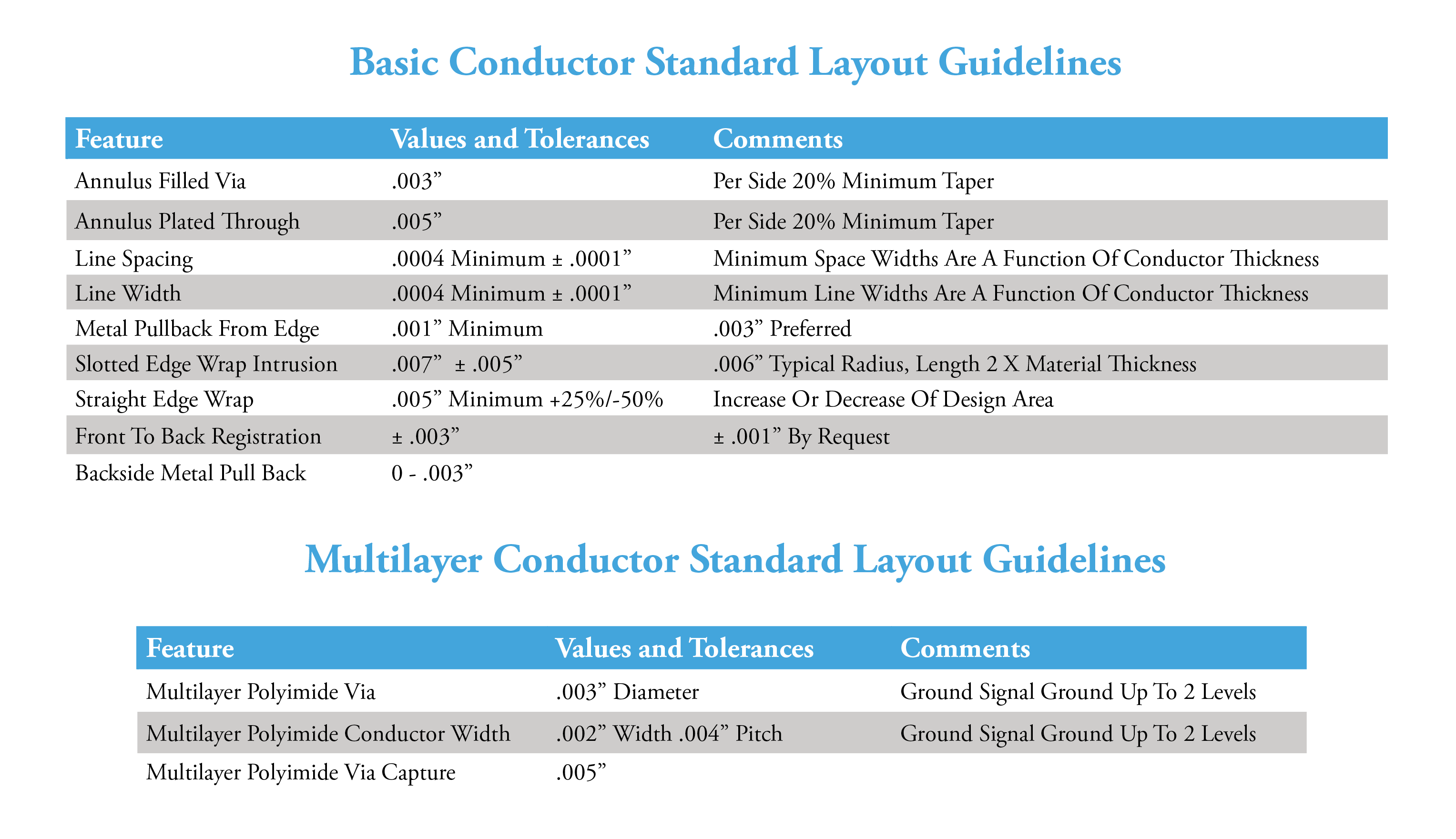
Conductor Dimensions for Standard and Multi-Layer Conductors
All circuit designs contain critical dimensions necessary for compliance and performance. It is important to consider these dimensions when designing the circuit to avoid adding unnecessary costs to the design. It is also important to note that conductor tolerances of <0.001" require more costly tooling to ensure compliance.
 While many organizations use the same metallization on every product because "that's how it's always been done," as part of our build-to-print process, we believe that it is best to consult with the sales engineer or factory regarding the options available to meet your specific requirements. This extra discussion will always result in the optimum metallization for your specific application.
In the next post, we cover how we approach laser machining for resistors with tight tolerances and hard-to-fit parts with profiles that are not geometrically square. In the meantime, you can check out the rest of our Build-to-Print Basics series posts to learn more about our build-to-print and thin film offerings or download the comprehensive Build-to-Pring Ebook.
