

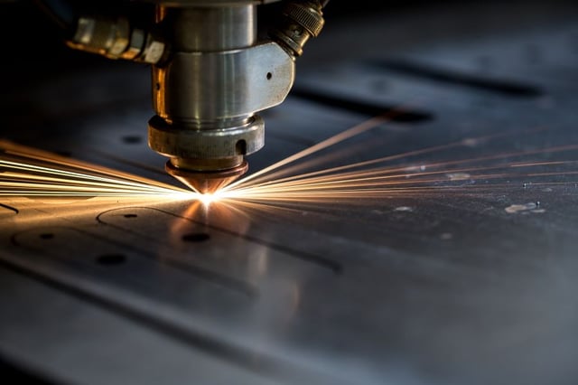
To provide a better understanding of build-to-print in general and the breadth of our offerings, as well as how our thin-film technology can benefit your applications, we’ve put together a Build-to-Print Basics series. Part 7 covers how we use in-house laser machining, laser trimming, and other laser cutting techniques to build high-precision thin-film components.
At this point in the build-to-print process, you’ve already determined the best substrate material and metallization scheme for your application. Now it’s time to establish the best processes to use to make everything all physically fit together and function appropriately. The following laser cutting techniques, from least to most precise, may be required for your project:
- Laser scribing – The ceramic substrate is perforated by the laser so the customer can break apart the ceramic at the appropriate point when ready to use.
- Laser machining – Used to cut the ceramic materials to make the “puzzle pieces” that form each plate.
- Laser trimming – A high-precision technique where lasers are used to carefully remove small bits of resistive metallization on the ceramic to make final adjustments to bring the part into spec. This includes techniques such as plunge, scan, and serpentine cuts.
- Laser obliteration – This is similar to laser trimming but can remove gold, nickel, and copper to achieve high-precision tolerances.
Before jumping into more details on these techniques, let’s first look at the different lasers that can be used for these processes. In general with lasers, the smaller the wavelength, the more capable it is of performing high-precision cuts. Therefore, the following three types of lasers can be used to perform different jobs – CO2, fiber, and UV lasers.
Starting with the CO2 laser, invented in 1964, this is one of the oldest types of gas lasers. Because it offers high power and is relatively low cost, it is a common laser machining workhorse. Similarly, fiber lasers use doped fiber as the gain medium. These lasers are also high power and can offer a range of wavelengths, and therefore different precision compared to the CO2 lasers. And finally, UV Lasers, as the name implies, operate at much smaller wavelengths compared to CO2 and fiber lasers. This means UV lasers offer much tighter control over feature size, making them ideal for very precise and tiny cuts, like those needed for laser trimming and obliteration.
A Closer Look at the Various Laser Techniques
As mentioned, laser machining is the process used to make initial cuts to the substrates used to make thin-film devices. At Knowles Precision Devices, we recommend following the guidelines outlined in Table 1 for laser machining.
|
Property |
Value and Tolerances |
Comments |
|
Maximum Thickness |
.060" |
Thicker materials require factory consultation |
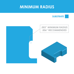 |
.003" |
CO2 beam width = .003", use .006" min. radius to change cut direction |
|
Smallest Feature |
0.6:1(ratio) minimum diameter |
|
|
Front-to-Back Taper |
10 – 15 percent of material thickness |
Includes bell effect at entrance |
|
Via Hole for Plated Thru Connection |
0.8:1 (ratio) hole diameter to material thickness |
Measured at exit, account for metal annulus on circuit side |
|
Via Hole Filled |
0.7:1 (ratio) hole diameter to material thickness |
Account for metal annulus on circuit side |
|
Feature Size Tolerance |
± .002" |
Non-cumulative |
|
|
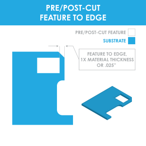
1X material thickness |
Not less than .020" |
 |
1X material thickness |
Not less than .020" |
|
|
± .003" |
All cutouts require a .003" pullback of backside metal |
|
Diamond Sawing |
± .001" min |
± .002" Standard |
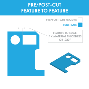
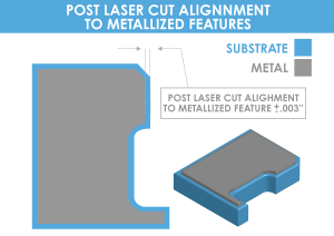
Table 1. These are our recommended guidelines for holes machined features using laser machining techniques.
When working on your thin-film design, it’s a good idea to discuss requirements such as feature spacing, minimum radius, and via taper with your applications engineer. Additionally, our engineers can perform some unique laser machining processing that you should be sure to discuss with your applications engineer as well.
Similarly, Table 2 shows the laser scribe specs we recommend following.
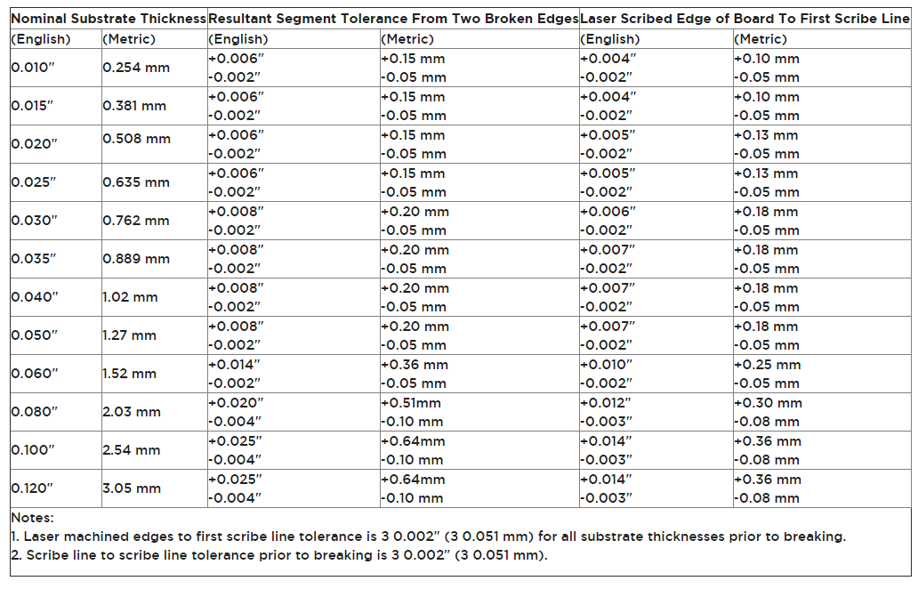
Table 2. These are our recommended guidelines for laser scribing.
For applications where resistors have tighter tolerances below our standard bake-in tolerance of ±10 percent, we have resistor trimming available. This could include high-volume throughput for chip resistors, attenuators, and complex circuits. Plunge cut, scan cut, microwave scan cut, ladder networks, and "copy trim" are all aspects of laser trimming that can be incorporated into a design for tolerances as small as 1 percent. Additionally, laser cutting is available for areas within the part that need to be removed such as location pins or hard-to-fit parts with profiles that are not geometrically square.
Knowles Precision Devices Has In-House Laser Expertise
At Knowles Precision Devices, we understand that lasers do not operate uniformly across materials. It takes a lot of know-how and craftsmanship to drive these lasers to precisely machine thin-film components. Not only do operators need to know how to use the lasers, which takes a unique skill set in itself, they also need to have an in-depth understanding of how the laser beams will interact with the different materials.
This is why we don’t outsource this work. We have the expertise to perform all the above-mentioned techniques with the appropriate lasers in-house in our extremely precise machine shop. Our precision machinists know how to get things just right on the wide variety of materials we work with. These are critical skills for building components with tight tolerances and hard-to-fit parts with profiles that are not geometrically square.
In the next post, we will cover conductor tolerances and design guidelines. In the meantime, you can check out the rest of our Build-to-Print Basics series posts to learn more about our build-to-print and thin film offerings or download the comprehensive Build-to-Pring Ebook.
