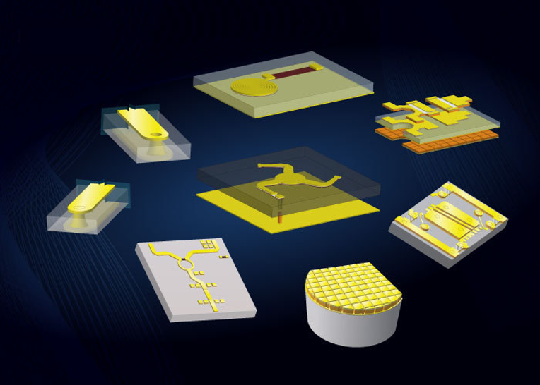
As a manufacturer of custom ceramics for thin-film circuit development for more than four decades, we are highly familiar with all the complexities involved in working with these materials to build a variety of circuits. Over the years, we’ve received quite a few questions about this technology, so we put together this Q&A to help answer some of the common questions you may have about thin film circuits.
Heterogeneous Integration for Electronics Design in RF and Microwave
Heterogeneous integration (HI) refers to the process of combining a set of electronic components with different functions and material compositions into a single, compact system. Particularly in radio frequency (RF) and microwave applications, HI-based designs accommodate higher functional density and better performance when implemented with application-specific requirements in mind. Integrated Passive Devices (IPDs), like conductors, resistors, vias, traces, and bridges, play a significant role in HI because they’re largely responsible for the resulting performance optimization when components combine.
Topics: Build to Print
Leveraging Thin Film on Ceramic Substrates for Interconnects and Interposers
Innovation in advanced packaging was driven, in part, by advancements in interposer design and construction. Interposers are electronic components designed to sit within a package and connect different circuits and components via interconnects. Thin film interconnects are standard in high-frequency components and subsystems where transmission line widths are small (i.e., .005” and under) to improve overall system performance. They also support high-power applications where thermal conductivity is more of a concern and certain materials like beryllium oxide and aluminum nitride are more commonly used.
Topics: Build to Print
Thin Film Integrated Passive Devices at Knowles Precision Devices
Resistors, inductors, and capacitors are the most common passive electronic components; they’ve long been available at different price points with different capabilities. Heightening expectations for performance in today’s advanced electronics environment mean we need equally advanced processes for creating components.
Topics: Build to Print
Build-to-Print Services for Thin Film Circuit Design and Construction
As the name implies, “thin film” is a precisely deposited layer of material used to fabricate electronic components. “Thin” can mean as little as a fraction of a nanometer thick. Circuits constructed with thin film are used in a wide range of electrical and optical applications, but they are most advantageous when high-frequency performance, tight tolerances, thermal conductivity, and long-term reliability are paramount concerns. Particularly in the high-frequency microwave space, small size, line definition, and repeatable construction offer significant performance benefits.
Topics: Build to Print
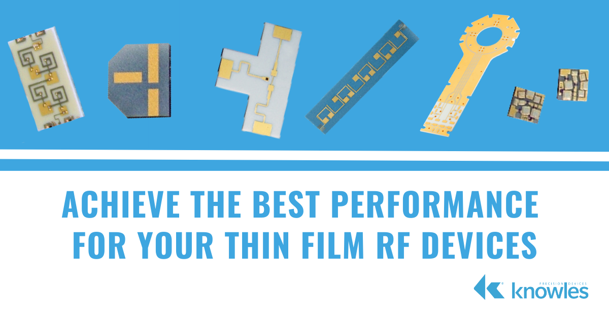
Achieve the Best Performance for Your Thin Film RF Devices
As the demand for faster communications across consumer and commercial devices continues to increase, operating frequencies of RF devices are being pushed higher and higher. This creates a number of challenges for RF device designers, as filter size must be reduced to compensate for smaller device sizes and shorter wavelengths while also maintaining high levels of performance. While surface mount technology (SMT), and in particular microstrip implementations, are an excellent option to meet these demands, it is important to note that not every SMT microstrip filter is created equal. There are a variety of choices to discuss with your filter supplier, such as substrate type, plating technology, and topology that can dramatically reduce the size and increase the performance of an SMT microstrip filter. One particular choice that Knowles Precision Devices has guided customers through for decades is the decision to use thin film for these filters.
Topics: RF and Microwave, Filtering, Build to Print
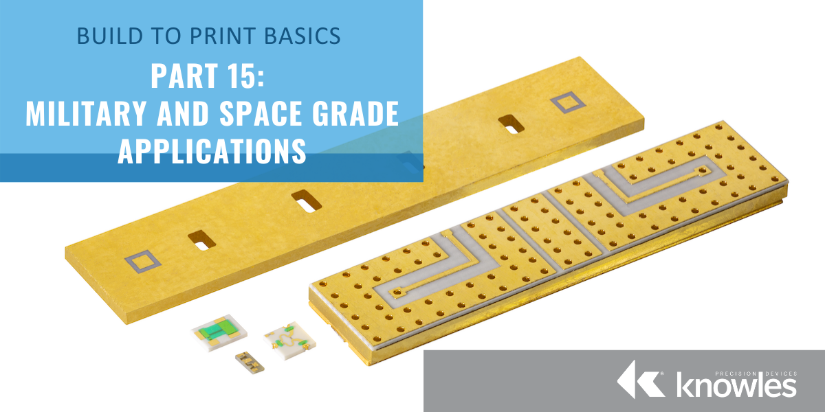
Build-to-Print Basics Part 15: Military and Space Grade Applications
To provide a better understanding of build-to-print in general and the breadth of our offerings, as well as how our thin-film technology can benefit your applications, we’ve put together a Build-to-Print Basics series. In this final post of our Build-to-Print Basics series, we discuss the quality standards we follow to ensure our components are qualified for military and space grade applications as well as the additional testing or spec design we can perform as needed by our customers.
Topics: Military and Aerospace, Build to Print
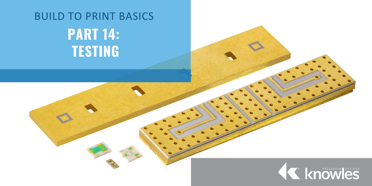
To provide a better understanding of build-to-print in general and the breadth of our offerings, as well as how our thin-film technology can benefit your applications, we’ve put together a Build-to-Print Basics series. In part 14 we discuss a range of non-standard testing services our facilities can provide when needed by our build-to-print customers.
Topics: Build to Print
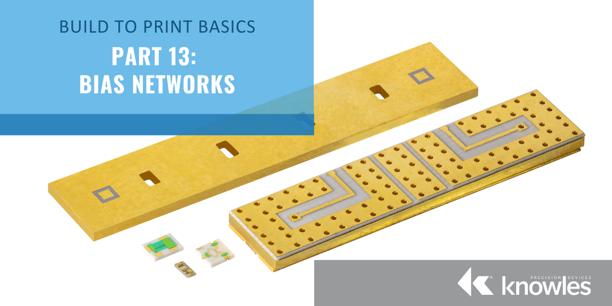
To provide a better understanding of build-to-print in general and the breadth of our offerings, as well as how our thin-film technology can benefit your applications, we’ve put together a Build-to-Print Basics series. In part 13 we provide an overview of how we use our build-to-print process and thin-film expertise to develop bias networks that support the functionality of active microwave components while also minimizing the space needed in a circuit for certain components and simplifying circuit assembly.
Topics: Build to Print
Build-to-Print Basics Part 12: Custom Microwave Components
To provide a better understanding of build-to-print in general and the breadth of our offerings, as well as how our thin-film technology can benefit your applications, we’ve put together a Build-to-Print Basics series. In part 12, we tie everything we’ve discussed so far together and provide more specifics about how we use the processes and options detailed throughout this series to create the custom microwave components you need.
Topics: RF and Microwave, Build to Print

