

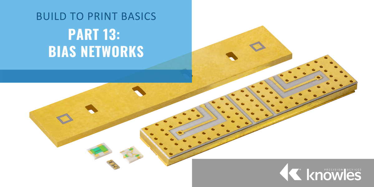
To provide a better understanding of build-to-print in general and the breadth of our offerings, as well as how our thin-film technology can benefit your applications, we’ve put together a Build-to-Print Basics series. In part 13 we provide an overview of how we use our build-to-print process and thin-film expertise to develop bias networks that support the functionality of active microwave components while also minimizing the space needed in a circuit for certain components and simplifying circuit assembly.
In our previous post in this series, we discussed a variety of passive microwave components, or integrated passive devices (IPDs), that we can design and develop as part of our build-to-print services. In this post, we expand on this with the details of a type of IPD, the bias network, that is commonly made with thin-film processes but used to support active microwave components such as amplifiers.
To start at the beginning, as you likely know, biasing is the process of getting DC voltage from point A to point B in the most appropriate way in a circuit. A bias network assists with this by combining capacitors and resistors in a specified way to best meet the specific needs of the device where the circuit will be used. To make a bias network, the necessary components are fabricated on the same substrate. This means that this section of the circuit can be ‘abstracted’ out as a single component, which saves on space and assembly cost.
Three of the most common types of bias networks are the bias filter network, the self-bias network, and the bias tee. While we can fabricate bias tees using our build-to-print process if a customer brings us a design, we mainly focus on developing bias filter networks and self-bias networks with experience frequently working all the way up to 67 GHz. Let’s explore the development and functionality of these two bias networks in more detail.
Bias Filter Networks
A bias filter network can be used for biasing when it is necessary to remove noise when getting DC voltage from point A to point B in a circuit. We can design our bias filter networks for high-performance microwave applications in a surface mountable package using a combination of our temperature-stable, high-permittivity dielectrics with our thin-film processing expertise. Therefore, our bias filter networks are ideal for filtering noise from supplies and reducing RF feedback in wireless communication and high-gain RF/microwave modules. Additionally, our bias filter networks can simplify assembly and reduce the size, weight, and power (SWaP) of a circuit as one component can be used to replace many small components. An example bias filter network is shown in Figure 1.
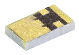
Figure 1. An example of a bias filter network we developed.
Self-Bias Networks
Self-bias networks are used to integrate source decoupling and user-selectable bias resistance. In other words, self-bias networks are used to get the current “just right” for amplifiers. To meet our build-to-print customer’s needs for self-bias networks, we combine our high-permittivity ceramics with our expertise in thin-film resistors to provide a device that integrates source decoupling and user-selectable bias resistance. The self-bias networks we develop using this process can improve gain flatness and stability in GaAs field-effect transistors (FETs). Like our bias filter networks, self-bias networks can also simplify assembly since one component can be used instead of many and the SWaP of the circuit can be reduced. For example, self-bias networks used as a pair can replace two standard parallel plate capacitors and a separate set of bias resistors, reducing parts count, assembly, and size. Figure 2 shows an example of a typical self-bias network.
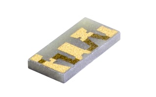
Figure 2. An example of a self-bias network we developed.
At Knowles Precision Devices, we not only have the capabilities to use thin film in the most appropriate way to develop the right bias network for your specific needs, we also have the expertise to ensure our these components are installed in a circuit in the most effective way. For example, with both bias filter and self-bias networks, we know these components should be mounted with the fully metalized side down directly on the RF ground plane for maximum isolation performance.
In part 14 we will review the testing capabilities we can offer our build-to-print customers. In the meantime, you can check out the rest of our Build-to-Print Basics series posts to learn more about our build-to-print and thin film offerings or download the comprehensive Build-to-Pring Ebook.
