

To provide a better understanding of build-to-print in general and the breadth of our offerings, as well as how our thin-film technology can benefit your applications, we’ve put together a Build-to-Print Basics series. In part 12, we tie everything we’ve discussed so far together and provide more specifics about how we use the processes and options detailed throughout this series to create the custom microwave components you need.
Throughout this series, we’ve talked a lot about the processes we follow and options we make available to our customers – from substrate selection to via designs – through our build-to-print process. While it’s clear we can customize basically every part of a circuit, you may be wondering, what components or devices can we actually design and develop for customers using these processes and our expertise? Let’s explore the possibilities in this post.
Working with Different Types of Planar Transmission Lines
In general, our build-to-print process and thin-film technology are ideally suited for designing and building components and microwave integrated passive devices (IPDs) based on planar transmission lines, which are conductors, or in some cases dielectric strips, that are flat ribbon-shaped lines. There are several types of planar transmission line designs we can use, but for simplicity, let’s focus on how we use microstrip, stripline, and coplanar waveguides for the devices we build.
First, let’s look at microstrip transmission lines. These transmission lines consist of a conducting strip separated from a ground plane by a dielectric substrate (Figure 1). With microstrip technology, entire components such as antennas, couplers, filters, and power dividers are formed from metallized patterns on the substrate. By using a microstrip approach with our high K materials on high-precision thin-film photolithographic technology, components can be made lighter, more compact, and typically less expensive than what is possible with alternative transmission line technologies. This approach inherently reduces size, weight, and power (SWaP).
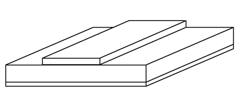
Figure 1. A drawing of a microstrip configuration.
Although stripline is similar to a microstrip approach, a stripline transmission actually lines use a flat strip of metal sandwiched between two parallel ground planes with the insulating material of the substrate forming a dielectric (Figure 2). With a stripline approach, coupled line structures do not need compensation for unequal phase velocities like those that can occur in microstrip. Also, there is less radiation using stripline, but the Q, manufacturability, and tolerance all decrease with stripline versus microstrip, which means this method is not as good of an option for applications that require higher Q and tighter tolerances.
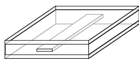
Figure 2. A drawing of a stripline configuration.
Lastly, a coplanar waveguide uses a single conducting track printed onto a dielectric substrate with a pair of return conductors on either side of the track (Figure 3). Like a microstrip configuration, coplanar waveguides can have active devices mounted on top of the circuit, although this configuration will generally not be as compact as a microstrip. Additionally, since a coplanar waveguide does not have parasitic discontinuities in the ground plane, this configuration can provide an extremely high frequency response of 100 GHz or more. This makes coplanar waveguides a good fit for monolithic microwave integrated circuit (MMIC) integrated circuit (IC) devices that operate at microwave frequencies.
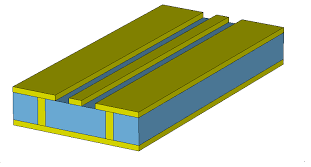
Figure 3. A drawing of a coplanar waveguide configuration.
Building Custom Microwave Integrated Passive Devices
In addition to building individual components with transmission line technologies, we also excel at building microwave and multi-stage components such as Lange couplers, Wilkinson power dividers, and hybrid bypasses. As discussed in Part 11, we understand how to properly connect a variety of components using solder and connected bridges where appropriate. Thus, we can reliably integrate a variety of components such as conductors, resistors, plated vias, selective high-conductivity traces, integrated resistors, filled vias, bridges, and transmission line structures, into a single IPD. Figure 4 shows examples of some IPDs we have created for customers.
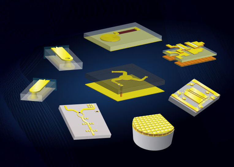
Figure 4. A sampling of IPDs, including a spiral inductor, interposer, and a power divider, that we are capable of making.
More complex integration between transmission line elements and discrete capacitor, resistors, and inductors to create IPDs is not an easy task. If this is not done correctly, condensing multiple passive components into a small device can lead to a number of issues. At Knowles Precision Devices, we excel at this. First, we offer a variety of High-K substrates that are ideal for circuit miniaturization using our thin-film process. And second, as we said in part 2, “The marriage of ceramic expertise, manufacturing know-how, product quality, customer service, product customization, and clever microwave and RF design engineering allows us to offer this variety, while many of our competitors cannot.” In short, we know how to use thin film with our proven build-to-print process to make things work the way they are supposed to.
In part 13 we will discuss bias networks. In the meantime, you can check out the rest of our Build-to-Print Basics series posts to learn more about our build-to-print and thin film offerings or download the comprehensive Build-to-Pring Ebook.
