

To provide a better understanding of build-to-print in general and the breadth of our offerings, as well as how our thin-film technology can benefit your applications, we’ve put together a Build-to-Print Basics series. Part 11 covers how we work with solder, solder masks, and supported bridges in the thin-film components we design and develop.
You can have a beautifully designed circuit, but if you can’t reliably connect the various components within the circuit, your beautiful design is negated. Let’s look at some of the materials and techniques Knowles Precision Devices uses for soldering and bridging, and how we handle these techniques as circuit complexity increases.
Soldering Options
As we touched on in part 6 on metallization, the solder layer and any corresponding necessary solder barriers, are an important part of any circuit design. Previously, solders containing lead were commonly used, but in recent years the elimination of lead from electronic devices as mandated by the Restriction of Hazardous Substances (RoHS) directive is driving a transition among many circuit designers regarding the materials needed for the solder layer. Thus, Knowles Precision Devices offers pre-deposited and patterned Au/Sn solder. On designs with multiple solder hierarchy or multiple pre-form sites, this can be a cost-effective method for eliminating pre-forms.
More specifically, our Au/Sn eutectic is a sputtered material (Au,80.4/ Sn,19.52 - Weight %, Typ); which provides superior flatness and thickness control. Typically, sputtered films can replace preforms of two to three times the thickness, helping keep circuits small. Sizing of Au/Sn pads is critical and is developed from customer supplied information with respect to die size and tolerance.
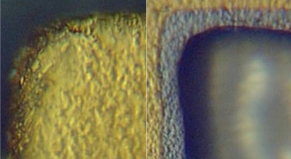 Figure 1. The image on the left shows a close up of the Au/Sn edge before reflow, and the image on the right shows the Au/Sn after solder reflow.
Additionally, while Tables 1 and 2 below provide an overview of the Au/Sn material properties, we recommend a consultation with our factory for more information on available thicknesses and other details for applications and design criteria. Other solders options beyond Au/Sn are available on request.
|
Au/Sn Eutectic Material Properties |
||
|
Parameter |
Value |
Units |
|
Composition |
80 Au / 20 Sn |
Wt % |
|
Melting Temperature |
284.0 |
°C |
|
Density |
14.5 |
g/cm3 |
|
Electric Conductivity |
7.7 |
%IACS |
|
Thermal Conductivity |
57.0 |
W/mk |
|
Temperature Coefficient of Expansion |
16.0 |
m/mK |
|
Resistivity |
160.0 |
n ohm m |
|
Modules of Elasticity |
59.0 |
GPa |
|
Tensile Strength |
276.0 |
MPa |
Table 1. The eutectic material properties of the Au/Sn solder we use.
|
Integrated Au/Sn (80/20 wt %) Eutectic Solder |
|||
|
Feature |
Value |
Tolerance ± |
Comments |
|
Thickness range |
80 - 200 µ" |
20 µ" |
Most common thickness = 160 µ" |
|
Minimum feature size |
.005" |
N/A |
|
|
Solder pad pullback from Au metallization |
.0015" |
N/A |
Eutectic pad is inboard of conductor |
|
Au metallization pullback from substrate edge |
.002" |
N/A |
Termination at edge is available, consult factory |
|
Solder pad placement |
N/A |
.001" |
|
|
Minimum substrate thickness |
.005" |
N/A |
|
Table 2. This table shows the properties of the integrated 80/20 Au/Sn eutectic solder we use.
Protecting Other Components in Your Circuit with Solder Masks/Dams
When using solder in a circuit, a solder mask or dam usually needs to be incorporated. This is an area of non-solderable material applied to the patterned traces of a thin-film circuit to prevent solder from flowing away from surface-mounted components during solder reflow. Unwanted solder flow can cause surface-mounted components to move during soldering or cause solder joints to be thinner and/or weak.
At Knowles Precision Devices, we offer various solder masking options to suit the subsequent processing of the substrate. Our typical options include the following:
- TiW – We can provide a patterned TiW layer on the conductor surface to inhibit solder flow. This method is optimum for fast, lower temperature solders to restrict run out during reflow.
- Polyimide – We can provide patterned polyimide as a robust solder flow restrictor. With a thickness of 7um, polyimide can withstand higher temperature solders and provides a good, robust barrier to solder flow.
- Nickel Oxide – Using our in-house plating capability, an NiOx barrier is created by etching the top surface of gold exposing an underlying layer of Nickel and intentionally oxidizing the Nickel. The result is an extremely robust solder flow restrictor. Note that this method requires an additional conductor layer below the Nickel layer.
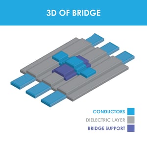
Making Connections with Supported Bridges
Today, many microwave circuits require the use of components such as Lange couplers to combine or split power or a spiral inductor for filtering and tuning purposes. However, when using traditional connection methods such as wire boding, these types of components can create challenges for the thin-film assembly process and are a common source of damage during manufacturing and testing. This is largely because the parasitic effects of some wire bonds make tuning and stable performance difficult, especially over broad frequency ranges.
Thus, when components such as a Lange coupler or spiral inductor are critical to a design, Knowles Precision Devices uses a connection option known as a supported bridge. Since we’ve used this method for quite some time now, we know it provides a consistent, reliable method for incorporating these structures into your designs. With supported bridges, we can also test the functionality of these components to ensure performance prior to integrating high-cost active devices. Table 3 shows the various features of our approach to creating supported bridges.
|
Feature |
Values and Tolerances |
Comments |
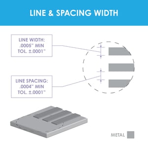 |
.0004" minimum ± .0001" |
Minimum space width available in TiW films only |
|
.0005" minimum ± .0001" |
Minimum line width available in TiW films only |
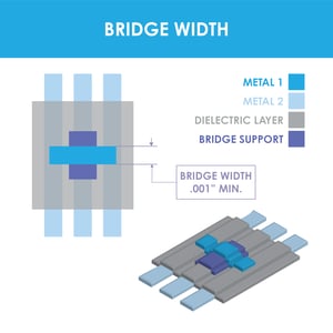 |
.001" minimum |
.0001" Bridge/Conductor Pullback |
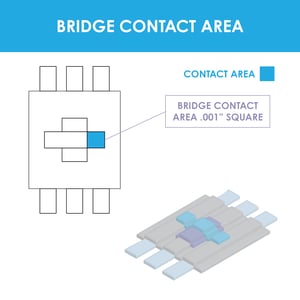 |
.001" square minimum |
|
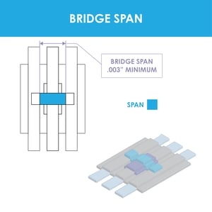 |
.003" minimum |
|
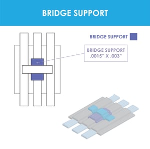 |
.0015" x .003" |
.0025" overlap, insulator to conductor |
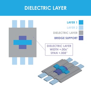 |
width + .006", span + .008" |
may be deleted at factories discretion on small bridges |
|
|
200 microinches minimum |
250 ±50 microinches typical |
|
|
250 microinches minimum |
300 ± 50 microinches typical |
 |
6:1 maximum |
|
In the next post, we will cover custom uW components. In the meantime, you can check out the rest of our Build-to-Print Basics series posts to learn more about our build-to-print and thin film offerings or download the comprehensive Build-to-Pring Ebook.
