

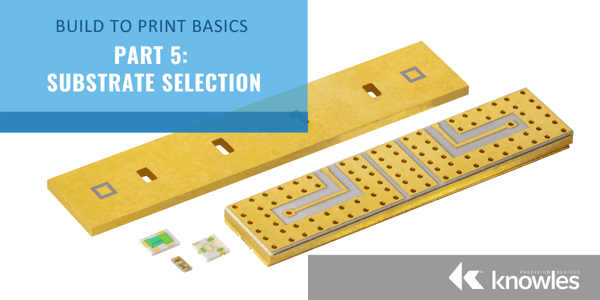
To provide a better understanding of build-to-print in general and the breadth of our offerings, as well as how our thin-film technology can benefit your applications, we’ve put together a Build-to-Print Basics series. Part 5 provides an overview of the common and custom materials we typically use and information on how we can work together to determine the best option for your application.
All circuit designs begin with the proper choice of substrate. As mentioned in part 4, Knowles Precision Devices stocks the most common substrate materials including Alumina, Aluminum Nitride, high-dielectric Titanates, Quartz, and Sapphire, and also produces a wide-variety of custom ceramics.
To determine the right fit for your build-to-print application, the following characteristics of the substrate material and your application that need to be considered:
- Operating frequency
- Size
- Dielectric constant
- Material type
- Thickness
- Transmission line impedance
- Mechanical requirements (TC, CTE)
Let’s start by analyzing the use cases and typical attributes of the five most common substrates used today in Table 1. You can also learn more details on the material properties of each of these substrates here.
|
Material |
Typical Uses |
Comments |
|
Alumina (Al203) 99.6% |
Low-to-medium power DC/RF microwave circuits using silicon or GaAs ICs standards. |
Cost-effective material with a wide range of applications. |
|
Aluminum nitride (ALN) |
High-power DC/RF/microwave circuits using silicon or GaAs ICs standards. |
Optimal CTE match with silicon devices |
|
Quartz (Si02) |
Microwave/mmWave circuits requiring extremely low loss or low CTE. |
Low loss tangent and CTE and a smooth surface finish. |
|
Titanates |
RF/microwave amplifiers or oscillators requiring High-Q resonators and transformers. |
Dielectric constants available from 12 to 100. |
|
Sapphire |
mmWave/optical circuits with special electrical or mechanical requirements. |
Low loss tangent and optical surface finish. |
Table 1. This table provides a high-level overview of common use cases and notable qualities for common substrates.
When it comes to these commonly used substrates, we can work with materials of a standard thicknesses from 10 to 40 mil in increments of 5 mil and offer surface finishes of “as fired,” lapped, or polished.
Using Knowles Precision Devices’ Custom Ceramics on Thin-Film to Significantly Reduce SWaP
As mentioned in part 3, in general, if you are building a circuit with size, weight, and power (SWaP) concerns, thin film is a good choice because it can reduce complexity and size while maximizing performance. Therefore, in addition to our extensive experience working with the five common materials noted above, we also produce a variety of custom ceramics.
In general, our custom ceramics offer the following benefits:
- Size reduction – Smaller and lighter systems
- Thin-film precision – Excellent repeatability and no tuning
- Improved field confinement
- Improved temperature stability
- Lower CTE mismatch stress in surface mount applications
- Reduced costs
More specifically, we offer a variety of High-K substrates that are ideal for circuit miniaturization using our thin-film process. Table 2 shows the properties of some of our custom high K materials alongside some of the most common standard materials.
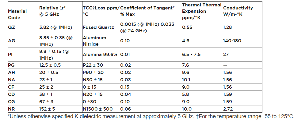 Table 2. This table provides an overview of the material properties for some of our most popular high K materials.
Finally, to help customers select the right material properties for their application, we’ve developed the following simplified process detailed in Figure 1.
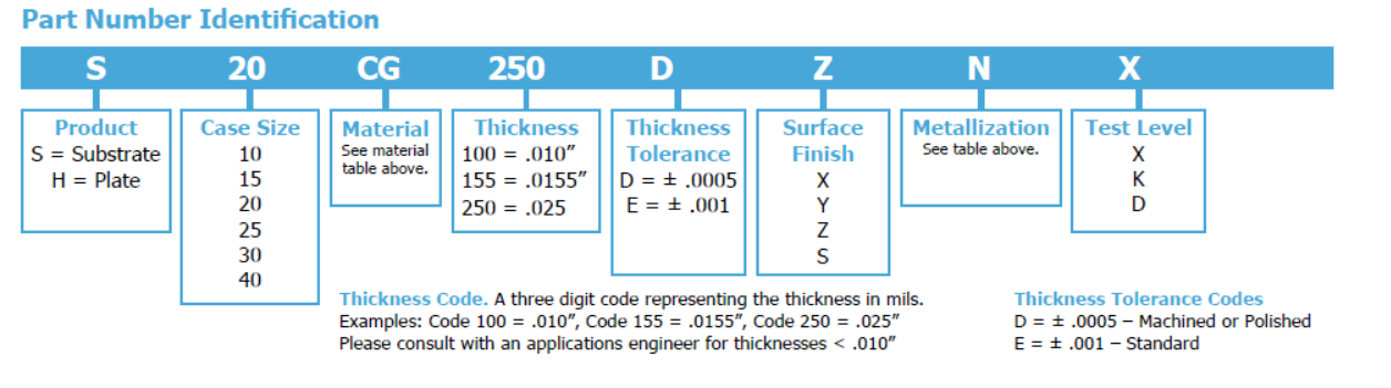
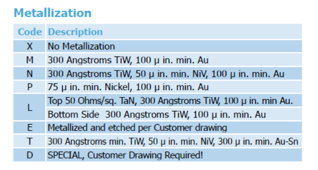
Figure 1. This is the process we use to work with customers to determine the most appropriate material choice for their build-to-print application.
In our next post, we will review the details on metallization. In the meantime, you can check out the rest of our Build-to-Print Basics series posts to learn more about our build-to-print and thin film offerings or download the comprehensive Build-to-Pring Ebook.
