

To provide a better understanding of build-to-print in general and the breadth of our offerings, as well as how our thin-film technology can benefit your applications, we’ve put together a Build-to-Print Basics series. Part 8 provides basic and multilayer conductor guidelines as well as information on fine line conductor features.
Basic Conductor Standard Layout Guidelines
|
Feature |
Values and Tolerances* |
Comments |
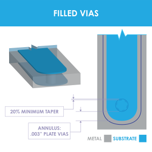 |
.003" |
Per side 20 percent minimum taper |
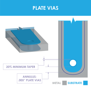 |
.005" |
Per side 20 percent minimum taper |
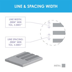 |
.0004 minimum ± .0001" |
Minimum space widths and minimum line widths are a function of conductor thickness |
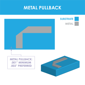 |
.001" minimum |
.003" preferred |
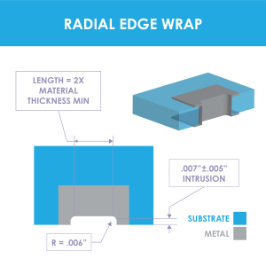 |
.007" ± .005" |
.006" typical radius, length 2x material thickness |
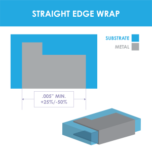 |
.005" minimum +25%/-50% |
Increase or decrease of design area |
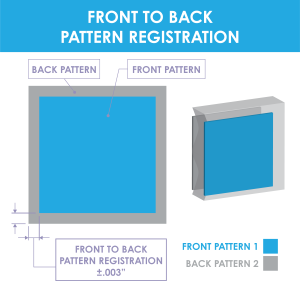 |
± .003" |
± .001" by request |
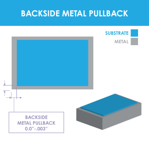 |
0 - .003" |
|
*Conductor tolerances of <0.001" will require more costly tooling to ensure compliance.
Multilayer Conductor Standard Layout Guidelines
|
Feature |
Values and Tolerances |
Comments |
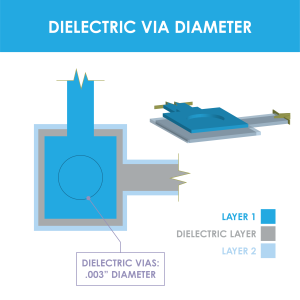 |
.003" Diameter |
Ground signal ground up to 2 levels |
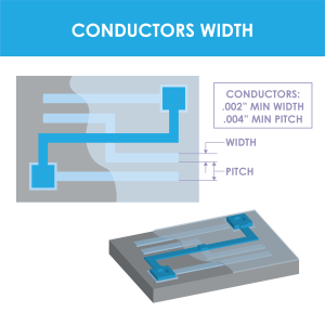 |
.002" width .004" pitch |
Ground signal ground up to 2 levels |
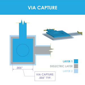 |
.005" |
|
Fine Line Conductor Features
Devices such as filters, diplexers, Lange couplers, directional couplers, interdigitated capacitors, and spiral inductors rely on the precision of conductor line width and line spacing to achieve targeted performance. As a result, there are a number of features that will vary depending on the line widths used in the conductor layer with various materials (Table 3).
Minimum Line Width and Conductor Spacing Tolerance
First, the characteristic impedance of transmission lines is governed by line widths. Next, the coupling between transmission lines and the control of the even and odd mode impedance to implement couplers and filters is governed by the line widths and the spacing between the adjacent transmission lines.
Additionally, the precise control of the spacing between the coupled lines ensures uniformity in voltage standing wave radio (VSWR) and coupling necessary to make coupler and filter performance repeatable. Edge acuity is also dependent on the thickness of the metal layers required, but generally is less than 0.1 mil. By selecting the proper substrate/metallization system, excellent edge acuity can be achieved and finished line widths will be within ±0.1 mils of the design dimension.
Finally, fine line width and line space geometries are impacted by the quality of the ceramic surface. Some materials used in thin-film products have grain structures and surface imperfections that may cause the loss of control of fine line widths and line space geometries. While polishing can be used to improve the quality of the surface, this technique is also somewhat limited since some materials do not hold up well to the forces created during polishing. However, one material that is not as limited is polished alumina. The surface quality is high and 1 mil line width/spacing is possible and repeatable when vias are present while 0.75 mil line width/spacing is possible and repeatable when vias are not used.
In the next post we will take a more in-depth look at vias. In the meantime, you can check out the rest of our Build-to-Print Basics series posts to learn more about our build-to-print and thin film offerings or download the comprehensive Build-to-Pring Ebook.
