Welcome to the Capacitor Fundamentals Series, where we teach you about the ins and outs of chips capacitors – their properties, product classifications, test standards, and use cases – in order to help you make informed decisions about the right capacitors for your specific applications. After describing dielectric polarization and losses in our previous article, let’s discuss five dielectric properties that affect capacitor performance.
Insulation Resistance
The perfect insulator has no movement of free electrons and possess infinite electrical resistivity. However, real-world insulators contain impurities and defects in their atomic lattice structure that give rise to charge carriers, resulting in some amount of leakage current under an applied electric field. Insulation resistance (also known as the parallel or shunt resistance of a capacitor) is a measure of the capability of a material to withstand leakage of current and is not the same as the series resistance of a capacitor. The insulation resistance of chip capacitors is dependent on the dielectric formulation, processing, and temperature at measurement (since resistivity decreases with temperature).
Using Ohm’s Law and the relationship of capacitance to geometry, we can demonstrate that capacitance and leakage current are directly proportional to one another. Since leakage current and insulation resistance are inversely proportional, it stands to follow that the capacitance of a capacitor is also inversely proportional to insulation resistance. Therefore, Electronic Industries Alliance (EIA) specifications establish minimum standards for insulation resistance (IR) as the product of the resistance (R) and capacitance (C), or RxC.
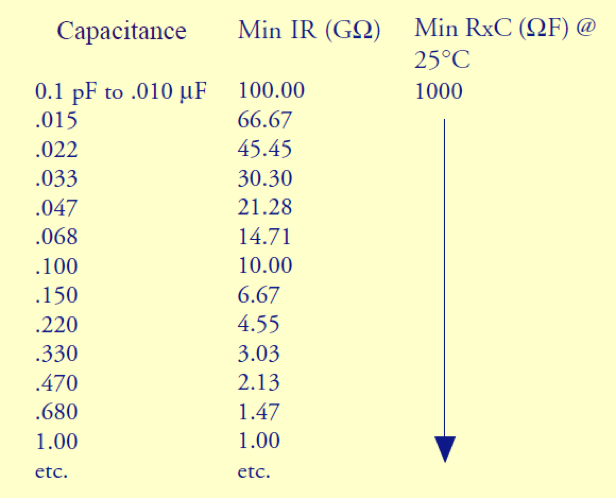
Figure 1. Minimum insulation resistance standards versus capacitance
In addition to material and geometric variables, insulation resistance is also affected by:
- Different resistivity at the dielectric’s surface, due to absorbed impurities or water moisture
- Physical defects in the dielectric formulation, which are proportional to the chip volume and complexity of its structure
Therefore, larger units (with larger electrode plate area and more numerous electrode layers) may possess a lower resistivity and thus lower insulation resistance than predicted for smaller devices.
Dielectric Strength
The dielectric strength is a measure of the material’s ability to withstand a large field strength without electrical breakdown, usually expressed in volts per mil (1/1000 of an inch) or volts per cm of dielectric. Dielectric failure occurs in insulators when the applied field reaches a threshold point where the restoring forces within the crystal lattice are overcome and an avalanche of free electrons is generated, resulting in a high burst of current that punctures the dielectric. In addition, high voltage stress creates heat and lowers the resistivity of the material, which may lead to a leakage path at the weakest portion of the dielectric.
The dielectric strength is diminished by physical defects in the microstructure of the material, and therefore the thicker the dielectric, the greater the probability of random defects and the lower the dielectric strength. Similarly, dielectric strength is inversely proportional to the electrode layer count of a chip capacitor and to its physical size.
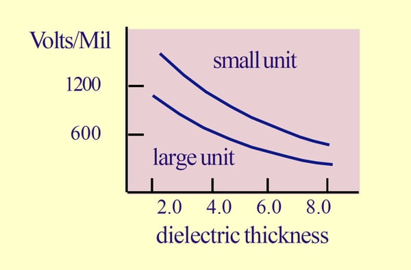
Figure 2. Dielectric strength versus dielectric thickness
Chip capacitors are designed with a margin of safety based on the above considerations to preclude failure in use and at the dielectric withstanding voltage test, which typically is 2.5 times the working voltage of the device.
Capacitor Aging
Ceramic capacitors made with ferroelectric formulations exhibit aging – which involves changes to the dielectric’s crystal structure caused by temperature and time. Ferroelectric materials exhibit spontaneous polarization, where dipoles naturally form without an applied electric field. However, over time the ions in the crystal lattice shift and stabilize to positions of lower potential energy. This degradation of the domains of polarization causes a logarithmic aging of the dielectric constant, such that the majority of capacitance loss occurs in the first 10 hours of age.
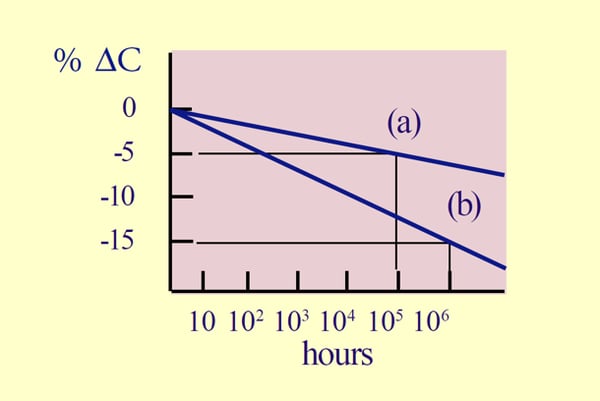
Figure 3. Ferroelectric aging, shown as percent change in capacitance over time
Aging in ferroelectric dielectrics can be reversed by bringing the material to a greater temperature than its Curie point (e.g. approximately ~130°C for barium titanate BaTiO3) and then cooling it back down. For example, this phenomenon can be observed shortly after soldering the capacitor, causing the dielectric to reform the domains of spontaneous polarization, recover its capacitance value, and recommence the aging process. Capacitor manufacturers compensate for capacitance loss of ferroelectric dielectrics by adjusting the testing limits, such that units do not age out of tolerance over a long time period.
Electromechanical Coupling
All dielectric materials display mechanical deformation or a change in shape when under the influence of an electric field. This behavior, known as electrostriction, is caused by ionic polarization (where the cations and anions within the crystal lattice are attracted to opposite directions) in crystals that have a center of symmetry. Electrostriction is a one-sided relationship because an electric field causes physical deformation, but applying mechanical stress does not induce an electric field (since the charged centers are not displaced).
Piezoelectric materials, on the other hand, display a two-sided relationship between mechanical stress and polarization. Because the crystals lack a center of symmetry, the centers of charge shift if the material is compressed, thus producing a dipole moment that results in polarization. This effect is a true linear coupling, as the elastic strain observed is directly proportional to the applied field intensity, and the polarization obtained is directly proportional to the applied mechanical stress.
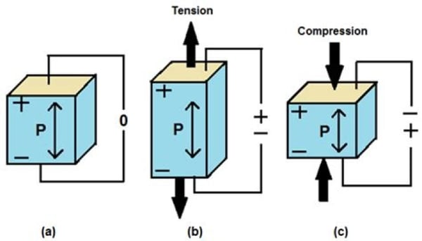
Figure 4. Different piezoelectric responses to applied mechanical stress (source: ResearchGate)
Dielectric Absorption
Dielectric absorption is the measurement of a residual charge on a capacitor after discharge, expressed as the percent ratio of the residual voltage to the initial charge voltage. This residual voltage is caused by the relaxation phenomena of polarization, covered in our previous blog post. Just as the polarization mechanisms can lag the applied field, the inverse situation also applies, where depolarization or discharge can also lag. In fact, a small fraction of the polarization may persist long after discharge, which can be measured on the device with a high impedance voltmeter. Dielectrics with higher dielectric constants, and therefore more polarizing mechanisms, typically display more dielectric absorption than materials with lower dielectric constants.
Hopefully, Part 5 gave you a better understanding of different dielectric properties and how they may affect your specific application. In Part 6, we’ll be diving into the unique characteristics of ferroelectric ceramics. Also, check out our Knowles Precision Devices Capacitors to view our complete product offering.
To learn more about capacitors, download our ebook, A Guide to Selecting the Right Capacitor for Your Specific Application.


