

To provide a better understanding of build-to-print in general and the breadth of our offerings, as well as how our thin-film technology can benefit your applications, we’ve put together a Build-to-Print Basics series. Part 10 covers our key design parameters for resistors as well as our standard layouts.
As discussed in post 6 on metallization, tantalum nitride (TaN) is the most common resistor material we use. This is because TaN offers higher maximum exposure temperature, a wider annealing window, superior resistance to the harsh environment encountered in soldering and other processing, and well-established self-passivating characteristics. For applications where minimum resistor change over temperature extremes is critical, we believe that nickel-chromium (NiCr) resistor films are a better choice. Table 1 shows the difference in performance for these two types of materials during 1,000-hour test.
|
Substrate |
Resistor |
TCR Range |
Sheet RHO |
Stability |
|
AI2O3, AIN |
TaN2 |
-125±25 |
25-150 |
<0.5% |
|
AI2O3 |
NiCr** |
0-25 |
50-250 |
<0.5% |
Note: All Tests are performed in forced air convection furnaces on un-trimmed resistors. **Proprietary Alloy
Table 1: Typical Resistor Data for 1,000 Hour Test at 125°C
Key Design Parameters for Resistors
When working on a build-to-print design, the key design parameters for resistors that we discuss with customers include resistor value, stability with time and temperature, and power handling. Additionally, the design of a thin-film resistor is governed by the following equation:
R = ρL/Wt
Where:
R = Total Resistance (Ω)
ρ = Bulk Resistivity of Resistor Material (Ω-cm)
L = Resistor Length (cm)
W = Resistor Width (cm)
t = Resistor Thickness (cm)
To ease design requirements, a parameter known as sheet resistivity (Rsheet), which is a measure of the resistance of thin films that are nominally uniform in thickness, is also considered. Sheet resistivity assumes L = W in the above equation, making the following equation apply instead:
Rsheet = RS = ρ/t (Ω/sq)
Therefore, simply multiplying RS by L divided by W yields the actual resistance, or
RTotal = Rsheet x L/W
Additionally, various sheet resistance values are available depending on the resistor range for the overall design.
While sheet resistivity selection should be left to the manufacturer when possible to maximize yield and reduce costs, when sheet resistivities must be specified, the overall range and tolerance requirements need to be balanced to obtain the optimum choice for processing. Some other considerations to note are that resistor tolerances of ±10 percent usually require trimming, although some designs can achieve ±5 percent without it. Resistor tolerances of less than ±2 percent will affect manufacturing yield in terms of the volume, and for resistor tolerances ≤ 1 percent, we recommend contacting our engineers for further design considerations to optimize yield.
Resistor Layer Implementation
The resistor metallization layer for all the resistors on a given circuit is deposited in a single sputter operation. Thus, resistors on a single part must share the same resistivity. We typically use 50 Ω per square for most designs. Table 2 below shows the standard resistor parameters for electrical design as well as allowable limits when using TaN.
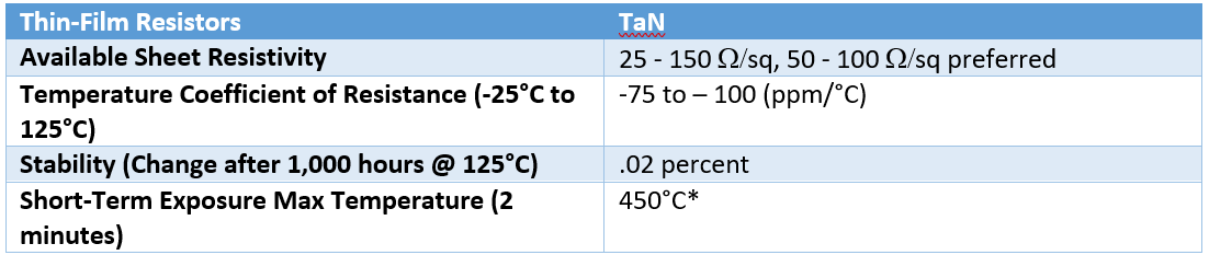
*If nickel is used in the system, drop exposure temperature to 350°C
Table 2: Standard Resistor Parameters
Finally, there are two fundamental resistor layout techniques we use – the notched resistor implementation and the flush resistor process (Figure 1). A general resistor layout guide is also shown in Table 3.
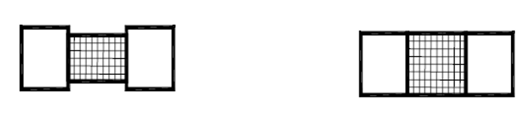
Figure 1. The drawing on the left shows a notched resistor process using an island method while the drawing on the right uses a flush resistor process with an etch-back method.
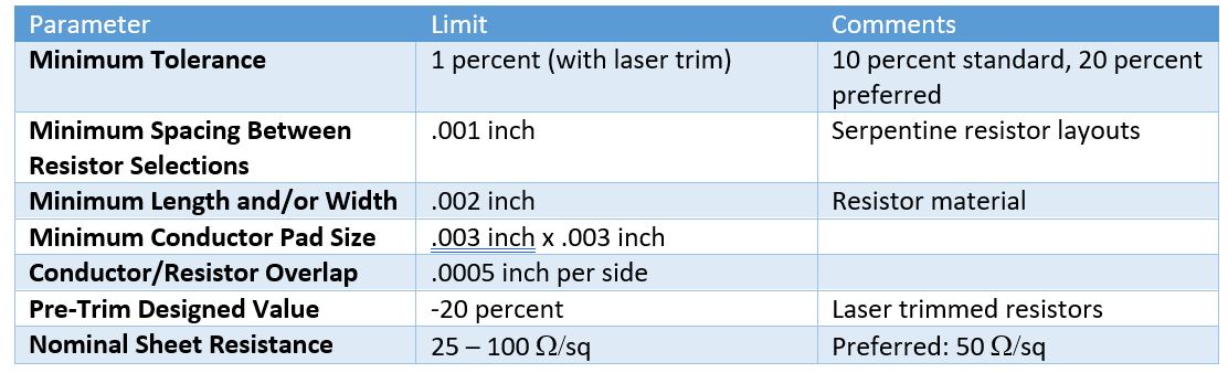
Table 3: Resistor Layout Guides
In the next post, we will cover how we use supported bridges as a consistent and reliable method for incorporating couplers and spiral inductors as well as how we use solder dams to provide the appropriate solder barrier. In the meantime, you can check out the rest of our Build-to-Print Basics series posts to learn more about our build-to-print and thin film offerings or download the comprehensive Build-to-Pring Ebook.
